Proximity Correction
Background
Proximity Effects are caused by electron scattering -- no matter how carefully you focus an electron beam, once it starts hitting a solid such as your resist or substrate, the electrons will scatter - they will head off in different trajectories than you wish. This is unavoidable physics. The result is that exposure is not the uniform binary Fully-Exposed or Fully-Unexposed that you would desire. Instead all edges are blurred by being somewhere in between full and zero exposure. Moreover, because the scattering range of electrons is quite large, the exposure an individual shape receives is affected by that shapes proximity to other nearby shapes in the pattern, thus giving rise to the name "Proximity Effects".
As an example, look at the e-beam exposed test pattern shown here. This is an optical microscope image, used because under-exposed resist shows up as different colors, so the effects are easier to see. While the center regions of the pattern are properly exposed, you can see that edge regions are under-exposed, and the degree of underexposure varies with the degree of isolation of a shape. So the edges of outer lines are underexposed, corners (which have less neighboring area) are more underexposed, and the narrow, isolated lines extending upwards are most severely underexposed.

Proximity effects causing underexposure in a test pattern. 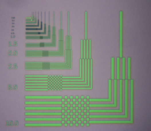
The same pattern exposed using Proximity Effect Correction to locally vary the dose to compensate for electron scattering.
An obvious question is why not simply increase the exposure dose so that all of the trouble spots in the uncorrected image above are properly exposed? This may in fact, work fine for many patterns and material combinations. But in many other cases, this will result in OVER-exposure of the central regions. So for example the checker-board like pattern areas will become over-exposed and the exposed squares will be much larger than the unexposed areas. Likewise, the central lines will be much wider than the edge lines.
Proximity Effect Correction
Fortunately, our LayoutBEAMER software has excellent proximity effect correction capabilities built in. In short, the software considers the effects of electron scattering and compensates for the effects by assigning varying local doses within the pattern.

Pattern with Proximity Correction applied. The color scale shows relative dose assignment varying over nearly a factor of 2 times, with the most underexposed areas in the above image getting the highest relative dose assignments.
Practical Proximity Effect Correction
As with most everything else in e-beam lithography, there are a dazzling number of variables and options when it comes to doing proximity correction. There are Dose Correction methods (as shown above) where dose is modulated to compensate for scattering. There are Shape Correction methods where the drawn size of shapes are modified to compensate. There are combination methods of these two. Within each method there are numerous options. Fortunately, in many cases, you can get significant improvement in your patterns using fairly basic, simple dose correction. If you have particularly difficult requirements, materials, or processing, you might have to do further tuning or more advanced techniques. As with most processing, though, you should start with the simple and only move to the more complicated cases as you need to.
I recommend you chat with the ebeam staff about your needs, as we have some considerable experience with these methods. I also recommend you read the LayoutBEAMER manual sections that cover their implementation of Proximity Effect Correction. Here I'll give you only a brief summary of one implementation of the process.
Electron Scattering
One piece of information you absolutely need to do any simulation or correction of proximity effects is a description of the electron scattering behavior. This is described using a Point Spread Function, giving energy as a radial function of distance from the point of beam incidence.

Scattering trajectories of just 200 electrons incident on 400 nm of PMMA resist on a Silicon wafer. Secondary electrons are shown in blue, while higher-energy Backscattered electrons are shown in red.
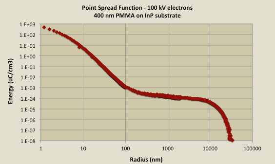
Example Point Spread Function for 100 kV electrons incident on a 400 nm PMMA layer on InP.
The Point Spread Function is often described using a mathematical fit, most commonly using a combination of 2 to 4 Gaussian functions, where each Gaussian is described by some half-width parameter, σ, of the form:

the Gaussians are then combined as shown in this equation:

where the parameters are:
- Alpha, generally representing the forward, or short-range scattering. of electrons heading into the material
- Beta, generally representing the backward, or long-range scattered electrons,
- Eta, the ratio between the energy in the backward Beta Gaussian to that in the forward Alpha Gaussian.
These parameters define the simple "Double-Gaussian" model, and just these two terms go a long way to adequately describing the electron scattering to achieve reasonably compensation for proximity effects.
It is also possible, however to include two additional Gaussian functions, which are generally used to represent mid-range, say 20-200 nm scattering where the double-Gaussian fit model doesn't always accurately fit the experimentally-measured scattering performance. In the case of 1 or 2 additional Gaussian functions, these are referred to as:
- Gamma1 and Gamma2, with their respectively energy scaling parameters are Nu1 and Nu2.
[Note: for some time, I had an incorrect normalization term in the form of the prototype Gaussian function above. This has now been corrected. My apologies. And then I found that my correction had two alpha terms and no beta term. Typos. Sigh. Hopefully I've really got it fixed this time for good.]
Sources for Point Spread Functions
Point spread functions depend most heavily on the incident electron energy, always 100 keV in our system, and the substrate materials. The resist material and thickness have a much smaller influence on the actual PSF, mostly because resists are generally all organic polymers with similar densities and average molecular weights.
1) Literature Search
This is without question the easiest way to find proximity parameters. If you can find someone else who has carefully evaluated proximity parameters for a process similar to yours, by all means I recommend you use those as starting values.
2) Modeling
There are various modeling software packages which do Monte Carlo modeling that claim to provide a good estimate of Point Spread Function if you give it a stack of material properties. In practice, these divide simply into two categories:
a) Expensive commercial solutions. Several companies sell electron scattering modeling software for typically well into the 5 figure dollar range. We don't have any of these.
b) Freeware solutions. There are at least two pretty-decent freeware simulations available. I have one of these, CASINO, installed on EBeam. Unfortunately, it's available only for Windows, so I have it running in a virtual machine on the ebeam workstation. It isn't all that easy to use or get a reliable fit, but I've made some progress. Talk with me if you think this might be useful.
Better than CASINO, though, is PENELOPE. This is based on very complex, older code (FORTRAN!), but has been shown to produce some of the best estimations of Point Spread Functions available, as it takes more physical phenomena into account, most notably, secondary electrons. Unfortunately, the licensing of PENELOPE is very restrictive, and the usage is downright ugly, requiring various configuration files be setup and then results extracted from those files in clumsy ways. Genisys provided (at one point in time) a front-end to make the setup, operation, and data extraction for a PSF from PENELOPE much more usable, but the licensing restriction on actually using the PENELOPE code remains. So if you want a PSF simulation, I have to run it for you, but it isn't all that difficult or time-consuming, so just talk with me about what material stack you intend to use, and I can probably provide a PSF as a simulation result.
New Jan 2014: A new possibility has emerged, in the form of a generally available simulation called pyPENELOPE. While not specifically geared toward extraction of a PSF, this may provide a way for you to use existing Monte Carlo simulation methods without the onerous licensing restrictions of the full PENELOPE package. Let me know if you try this out and what you find out.
3) Physical Measurement
This is by far the most difficult method, because accurately measuring the large number of very tiny feature sizes necessary to form an accurate model is very challenging in a research lab setting such as ours, where we don't own a multimillion dollar CDSEM. There are various publications that describe "easier" methods of characterization, including tasty concepts like the Doughnut Method, and a set of patterns designed to be "easily" imaged in an optical microscope, but even these methods turn out to be fairly challenging to get accurate values.
If your materials are truly unique, I have a pretty good collection of papers on this topic I'm happy to share with you, plus some experience of my own.
Tables / References
Here are some collected values that I know of:
| Material Stack | Alpha | Beta | Eta | Gamma1 | Nu1 | Gamma2 | Nu2 | Source |
|---|---|---|---|---|---|---|---|---|
| ZEP Resist 500 nm, on Si | 0.012 | 33.3 | 0.61 | Devin Brown, Ga Tech | ||||
| ZEP Resist 500 nm, on GaAs | .012 | 13.08 | 1.09 | Devin Brown, Ga Tech | ||||
| PMMA Resist 500 nm, on GaAs | .022 | 12.46 | 0.96 | 0.018 | 0.204 | 0.60 | 0.030 | LayoutBEAMER Sample |
Update: 2/2014. The newest release of LayoutBEAMER now provides a system library of PSFs in which I can add as I model new material stacks. Moreover, it's no longer necessary to fit the Gaussians to approximate a modeled PSF. Instead the PSF is represented as a numerical lookup for the simulated results.