E-Beam Process Overview & Basics
This section attempts to provide a high-level overview of the entire lithography process, with links to more details about each step.
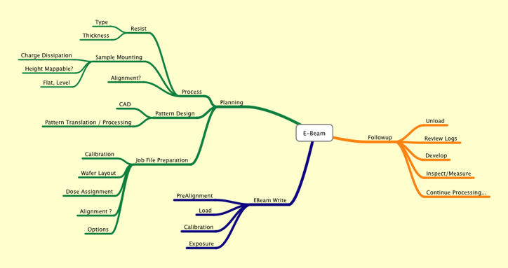
I’ve tried to map out the concerns and considerations you need to successfully expose a wafer with e-beam lithography with this diagram:
If you’ve never done any e-beam lithography before, you might want to take a look at some of these references to gain some initial familiarity.
Computers
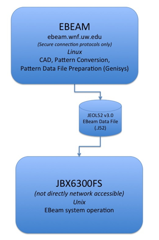
The vast majority of what you need to do to have a wafer written using e-beam lithography is computer-based work. You’ll need to use two different computers for any exposure; one computer is used to prepare the pattern data file for exposure, and the other computer actually runs the e-beam tool to perform the calibration, alignment, and exposure process. Some details on these two computers is shown in this figure:
Both computers you will be using are Unix/Linux-based, so you’ll need at least some minimal Unix and/or Linux knowledge. You won’t need to be a system guru, but you will need to be able to do:
- Basic file manipulations such as copying, renaming, making subdirectories,
- Edit text files (job and schedule files are required for each exposure)
- Display text files (to review the exposure log files after your job is completed)
I have a few notes about connecting to and using the computer named “EBEAM”, as well as some links to some introductory Linux/Unix tutorials.
Pattern Design & Preparation
Before you can write a pattern on the EBL system, you have to create your design data and get that data processed into a JEOL-specific data file. There are a few different pathways for doing this, but before you begin, you should be aware that even this simple-sounding step has numerous possible pitfalls that will result in you getting less-than-you-hoped-for on your final wafers. So you will do well to plan carefully before you even begin your design, and pay attention to details during your design and pattern preparation steps.
That primary data pathway is shown in this figure:
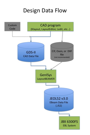
For most work, you will create your design in some CAD program. There are lots of programs available; they vary from simple freeware editors to full-blown IC design packages costing in the 6-figure range. What’s appropriate for your work depends entirely on your project needs. If you have any questions, talk with the e-beam staff; they can probably help you choose an appropriate option. For UW staff and students, the WNF maintains a site license for LayoutEditor, a very full-featured layout CAD package available for Linux, OS-X, and Windows. Look here for more information about LayoutEditor.
Independent of which program you use to design your pattern, you will almost always want to output your design data into an industry-standard data CAD data format called GDS-II (wikipedia), (usually pronounced Gee-Dee-Ess-Too). While this format is old and has some limitations for certain types of structures, it is the de facto standard, and nearly every fab house and mask shop uses this format. Other formats are possible, be each of these formats has their own peculiarities, and moreover, most of the other data interchange formats have various ambiguities and non-standard features that can cause your pattern data to not come out like your CAD program shows it. For maximum reliability and compatibility, use only GDS-II data format. See this page on Data Formats and Programs for more details.
GenISys LayoutBEAMER
UW has purchased the world’s leading software for preparing CAD data for e-beam writing, a package called LayoutBEAMER from GenISys, Gmbh. This is extremely powerful software with extensive capabilities, yet a pretty simple user interface. Data flows are setup using a simple flowchart interface. An example of a very simple data conversion looks like this:
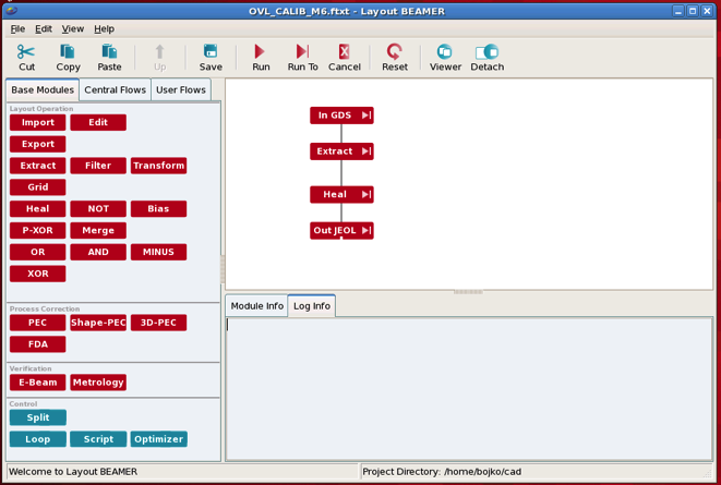
In this example, pattern data is read in from a GDS-II data file, a single layer of that pattern data is selected, and then the design data from that selected layer is output into a JEOL-format pattern data file. Don’t get too fooled by the simplicity though; there are multiple options and settings behind each of these data process modules, and having a wrong setting will likely result in a pattern file which either cannot be exposed, or will give you in writing results different from what you designed or desire. Go here for a lot more information about pattern preparation using GenISYS.
Sample Requirements
The e-beam system is flexible about what substrates it can expose on, but samples do need to meet all of these criteria:
- Compatible with a high-vacuum system: This means that the sample must be able to be cleaned of residual oils and organics by solvent cleaning, and must not show any significant outgassing in the vacuum of the e-beam exposure chamber.
- Can be clamped in a substrate holder: There are a variety of holders available, described in more detail here. They have some flexibility regarding exact shape and size, so check with me if you have a small chip sample.
- Electrically conducting: You’ll be putting 100,000 Volt electrons into your wafer surface; they need to have a conduction path to escape. If your samples are fully insulating, there are possible schemes that can be used for this purpose, for example using a very thin metal overcoating on top of the e-beam resist for charge dissipation.
So once you’ve got a sample that can work, it will need to be coated with electron sensitive resist.
Sample Preparation
OK, so assuming your sample meets all of the requirements, and you’ve got your pattern files ready to go, your next step is to coat your wafer with an electron-sensitive resist, such as PMMA or ZEP. This process proceeds almost identically to spinning and baking photoresist on your wafer, except that e-beam resist layers are typically much, much thinner than the photoresist layers you may be accustomed to using. For process details of the different resists we use, look here for process information.
JobFile Preparation
In addition to one or more expose-able pattern files, you will also need a set of job files which instruct the machine what conditions to use for your exposure, where and how to place your pattern files on your substrate, how to calibrate and align your patterns, etc. The jobfiles can be quite complicated themselves, so there’s a whole section dedicated to jobfile syntax and operation.
Exposure Process
At last, it’s time to expose your wafer. You need to load your sample into one of the e-beam holders which insures that the front face of your wafer is held level and at a height very close (within microns) of the calibrated focal plane of the e-beam deflection system. Then the holder, with your sample on it, is loaded into the system via a vacuum load lock. Once on the exposure stage, several calibration steps are performed to insure the beam is precisely calibrated for the exposure conditions you need to use. If you are not writing the first layer on your sample, and therefore the patterns you wish to write need to be aligned to patterns already on the wafer, then you’ll have to go through a wafer alignment procedure. In either case, the next step is to begin the exposure, which may last minutes or hours, depending on your pattern size and beam conditions. During this exposure time, there is actually very little for you to do. You can watch your pattern trace out on the computer screen, but really, there’s nothing much you can do now; it’s entirely under the control of the computer.
A whole lot more information about calibrating and exposing a wafer is found here.
After your exposure is completed, you must unload the holder from the e-beam system, again through the vacuum system load lock, and then unload your wafer from the wafer holder. Next, you develop your wafer in an appropriate developer solution. And then, assuming you got everything correct, you’ll have the patterns you designed in the resist layer on your wafer.
Prerequisites
If you want to do an e-beam exposure and would like to learn to use the e-beam system to do your own exposures, it will help you tremendously if you have some existing experience and skills related to microfabrication in general. The reality is that e-beam exposure work is more expensive and more demanding in almost every aspect than photolithography, so you should have some baseline experience before you attempt e-beam lithography. Here are some skills that you will need:
- Basic WNF chemical usage skills. You’ll need to use resists, developers, and strippers (solvent and bases). You’ll need to use the resist spinners, the baking hot plates, and general wet chemistry hoods.
- Basic WNF photolithography skills. It’s strongly recommended that you have some experience with photolithography, and interpreting the results of your work with an optical microscope.
- Optical Microscopy skills. You’ll pretty much always look at your patterns with an optical microscope, so you should be qualified and skilled at using one or more of the optical microscopes in the WNF.
- SEM skills. If you’re using e-beam lithography, it is most likely that what you are exposing is going to be too small to fully assess using optical microscopy, so you should be skilled with using an SEM. In addition, the manual beam calibration steps when operating the JEOL are very similar to obtaining a high-quality SEM image, so the more experience you have with this, the better your e-beam results will be. In particular, you may need to adjust the e-beam focus and astigmatism manually on the e-beam system, just like with an SEM, so this skill is required.