Design for E-Beam Exposure
When starting a design, it is important to take into account your expected exposure parameters BEFORE you begin design and layout. This is very important if you want to get the best results. Most typically, you’ll have to make some trade-offs between optimizing your writing and your layout. Here are a few specific issues you should be aware of in the planning process:
Grid Size
Fundamentally, everything our e-beam system exposes is based on a discrete, square Cartesian coordinate system, with all beam positions lying strictly at one of the X-Y grid points within the exposure field. For some patterns, the spacing of the fundamental grid points is insignificantly small. For others, careful design with consideration of the discrete nature of the grid points is essential for successful results. As a particular example, most photonic structures are critically sensitive to the grid point spacing; the round-off error, or “grid-snapping” that will occur if your design and the machine exposure grid are not coincident would ruin optical performance of many structures such as gratings.
The machine’s placement grid depends on which EOS mode you will be operating in. This is a very fundamental planning decision to be made early in your planning process.
You can find details on how the e-beam deflection system actually works, and how all of the gridding is embodied, here.
In practical exposures, you gridding will be some compromise of what the machine is capable of, what your design requires, and what the process can support. You will perhaps find that you cannot use as small a grid as you might like, because the system has an upper limit of pixel stepping speed, which equates to a minimum possible exposure dose for a given set of conditions. More details and some calculators including a “Minimum Dose” calculator, are here.
It’s always best to design your pattern from the start using the intended exposure grid. While it is possible to change the grid later, this can sometimes result in unintended consequences.
Gridding Error Example
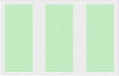
Have a look at this figure. It’s a pretty simple pattern, just three rectangles, shown in green shading -- that’s the pattern we want to expose. Each rectangle is the same size, 17 x 48 pixels -- let’s assume 4-th lens mode, so let’s say 17 x 48 nm in size, with an 8 pixel (=8 nm) gap between each rectangle. (In reality, our system almost certainly can’t resolve gaps this small; this is just an example where I was trying to make the effects visible to scale. -- the same gridding effects happen on larger-scale patterns too, they’re just harder to see in the drawing.)
So, if you want this pattern on your wafer, you draw this pattern in CAD, right? Well, maybe. But what will you get?
Now, let’s say we need to cover a larger area with this pattern, and we’re using PMMA resist. And so we choose beam conditions such that we will need to use a Shot Pitch of 4, or a 4 nm exposure grid spacing. Again, this is a hardware limitation that we simply cannot use a finer grid with the necessary beam conditions. But what happens to our pattern when we impose this 4 nm grid? Well, that’s the red dots. Do you spot anything wrong? Count the dots -- the left and right rectangles are written with 4 pixel points horizontally, while the center rectangle has 5 pixel points. That’s 25% more exposure in the center rectangle, and that is a huge impact to the resulting resist size. So if uniformity of size of your rectangles is important, you just failed, because the center rectangle will be larger than the other two.
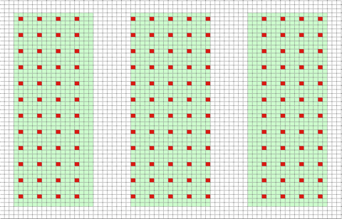
Is that all that’s wrong? No. Or, well, it depends. If the center position of each shape is critical, well, this gridding example failed in that case too. I’ve drawn vertical blue lines on these figures showing where I want the center of each shape to be. The center shape indeed has the center of its exposure coincident with the intended design center. But look closely at the left and right shapes. Because our exposure grid is not coincident with our design grid, neither the left nor right shapes have their center in the intended locations -- the center of the left shape is shifted one pixel to the left of intended and the right shape center is shifted to the right. Is a one-pixel offset in shape center significant? Well, that depends on your application, but the point remains -- applying an exposure grid on your shapes after design can cause your exposure to differ from your intended design, so you really need to be aware of exposure grid BEFORE you start your design to avoid these sorts of sizing or placement errors.

Field Boundaries
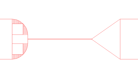
Another critical design factor is the placement of field boundaries. As described on this page, the e-beam system can only deflect the electron beam over a fixed area, which is called an e-beam field. Your pattern will be divided up into individual e-beam fields, with each field written sequentially. Because there is a stage move between the writing of adjacent fields, there will be some placement error between adjacent fields. While the system is very good at minimizing this stitching error, it is still finite, and might be large enough have a negative effect on your pattern writing. You can read more about the machine’s stitching errors here. Whenever possible, though, it’s best, and often possible, to avoid stitching errors entire through careful pattern design. Let’s look at an example. In this case, you want an array of simple nano-widgets, with a very narrow line connected by two large contact pads, like this:

Looks simple, but shown in this plot as thin grey lines are 500 um field boundaries, which would be the case if you were using 4th lens for an e-beam exposure. If you zoom in on the 3rd column of widgets, you’ll see this:
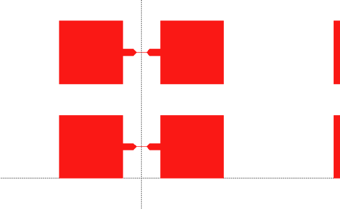
And we have a field boundary splitting our precious nanoline! If stitching errors were 0, this wouldn’t be noticeable, but here in the real world, we’re likely to see some combination of errors shown here:
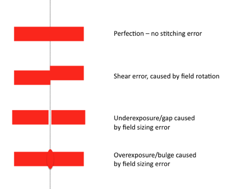
It’s hard to estimate exactly how bad stitching errors will be. When the system is well-calibrated, stable (low drift) and there are no sample charging issues, field stitching errors will be well under 10 nm. Does this matter? Again, this depends on the sensitivity of your design. A 10 nm error wouldn’t even be noticeable in a 10 micron feature, but might be a disaster to a 50 nm line.
What’s the solution? Simple: whenever possible design so that no critical features in your layout will cross field boundaries. Here are few hints how to achieve this:
- I usually create a dummy layer in my CAD design which consists of nothing but lines showing the location of e-beam fields. This allows me to place my devices so that they don’t span e-beam field boundaries.
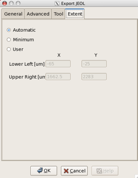
- You have to be very careful about field origin shifts possible during the pattern conversion process. LayoutBEAMER will, in automatic mode, place the J52 pattern origin at the upper left extent corner of your layout. This may or may not be where you intended the field origin to be. For many people, the lower left corner is a more intuitive origin. You can override this behavior with LayoutBEAMER’s Extent tab of the JEOL export options module.
- Always verify the placement of field boundaries in the data after fracturing. You can do this in LayoutBEAMER, or using JEOL’s “JBX Filer” software.
Shape Fracturing
If you look at how the system exposes shapes, you’ll find that everything is based on a square grid of exposure points. The system’s exposure sub-system processes only very simple, primitive shapes at exposure time. Your carefully-design CAD pattern will be fractured into numerous tiny shapes during the pattern processing step. Whether this matters to you or your pattern design again comes back to the same ambiguous answer: it depends. For many patterns, the shape fracturing will be entirely transparent, and the e-beam will be “what you get is what you see” on your CAD screen. For other designs, the nature of pattern fracturing may create headaches for you at expose time. Whenever possible, you should try to design your pattern with fracturing in mind. If possible, avoid using curves, and stick to straight line geometries. Even better, if possible, stick with 45 degrees geometries. Consider the example in this figure: one side is drawn as a curve, the other a polygon. As you can see, the curved side is fractured into a few dozen tiny shapes. Will this matter? Again maybe, maybe not. The system can certainly expose the curves, and most likely you won’t see any effects. The possible problems, though include:
- Poor shape butting. It is possible, mostly likely due either to poor system calibration or sample charging, that the little shapes on the left side might not align perfectly as designed. This might create a jagged or stepped edge along the edge of the curve.
- Large file size. If you have millions of curves, the size of the fractured data file can become excessive. Hard drives are big today, but not infinite. This is likely only a consideration for massive layouts with tiny curved shapes.
- Excessive shape overhead. System throughput, or writing speed, is always a concern in e-beam lithography, but the 6300FS system, for certain patterns, can exhibit excessive shape overhead that can cause your pattern to be multiples slower than you might expect, up to 7 or 8 times slower than you might predict. This is particularly the case for patterns containing billions of very shapes, such as fractured dot arrays of nano-dots. These patterns can still be done, but you might have to design a completely different way in order to avoid your write time taking 8 times than you want.
What’s the summary? When possible, simplify your designs. Don’t create extra complication when you don’t need to. Use simple, straight lines, even limit yourself to 45 degrees, when possible. Use other angles or curves when you need to, but be aware that increasingly complexity increases the possibility of errors creeping in.