E-Beam System Basics 1:
Beams, Fields, and Writing
This and the next few pages give you some background on how the e-beam system actually writes patterns, and introduces several key details you’ll have to understand to successfully design and write nanostructures with the e-beam system.
E-Beam Optics
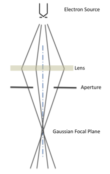
That’s a pretty simple diagram; this one is more realistic, showing far more of the electron-optical elements in our system, but you certainly don’t have to know this level of detail to use the system.

(Image from JEOL Documentation)
E-Beam Deflection
If all we did was get a small beam of electrons focussed onto the wafer surface, we’d have a machine that could make a dot in the resist, and that’s about all. The pattern “writing” ability of the ebeam comes from its “Deflection System”, which can “steer” that beam of electrons around the wafer surface, writing out a pattern that we’ve designed. In this simplified diagram, you can see how the electron beam can be positioned by the deflection electronics and electron beam deflector elements. Note that this is a digital deflection system, in which the beam positioning is determined by a digital value from the control computer, which is subsequently converted to an analog signal. As a digital signal, the beam positioning has a finite number of possible discrete values, as indicated by the dot outlines shown on the wafer plane in this drawing.

This fundamental digitization is very important; it underlies all operations, and is important to your design choices as well. Of course, our system is more complicated than this simple 1-dimensional diagram; of course we have 2-dimension beam deflection, so that we can trace out all sorts of interesting shapes. In operation, the system:
- Set the beam position to the location of the first desired exposed pixel of a shape
- “Unblanks” the beam, that is, starts hitting the wafer with electrons
- Pauses or Dwells for a define period of time to fully expose the resist at that pixel location
- Steps to the next pixel in the shape, and pauses to expose that pixel
- Repeats the previous two steps for every exposed pixel in the shape.
- Blanks the beam, to stop exposing the sample, so that the beam can then be re-positioned at the starting pixel of the next shape to e exposed.

This gives rise to a few fundamental concepts you should know about:
E-Beam Field and Machine Grid
First, an e-beam field is the amount of area the electron beam can scan across. In our system, each e-beam field has 2^19 bits in each axis, or 524,288 possible distinct beam positions, which are known in the JEOL system as “Shots”, although other common terms for these points would be “Pixels”, or “Machine Grid” points.
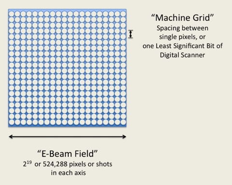
But exactly how big is an e-beam field? And how far apart are these shots? Well, our system has two possible operating modes:
Mode | Terminology | Field Size | Machine Grid Size |
| Higher-Resolution | 5th Lens Mode EOS Mode 6 | 62.5 um | 0.125 nm |
| Higher-Speed | 4th Lens Mode EOS Mode 3 | 500 um | 1.0 nm |
These numbers are important enough that you should try to remember them (or at least, remember where to look them up.) This data can be found most easily at the Quick Reference Page.
Vector-Scanning
This is a term used by e-beam folks to describe the writing strategy used in our system in which the beam is scanned only in the areas to be exposed, and then jumps from each exposed shape to the next, as in this figure:
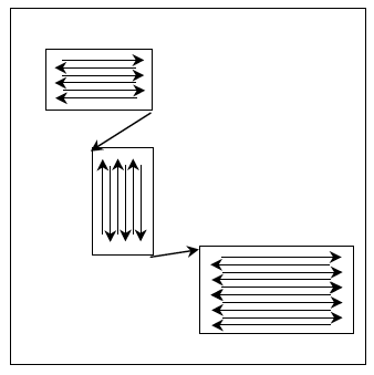
(Figure from JEOL Documentation)
This is contrasted with a different sort of e-beam system called a “Raster Scan” system, in which the beam is scanned over all surface area, being blanked and unblanked only in areas to be exposed. As a gross generality, Raster Scan systems scan at far faster rates, but are typically less accurate in beam placement, in particular in the case of alignment to existing layers. For very sparse patterns with little exposed areas, vector scan systems can be much faster than a raster scan system.
Field Stepping
Because of the fixed field sizes discussed above, any pattern larger than a single field must be written in segments, one field at a time, with the stage moving between adjacent fields between each, as shown in this figure:
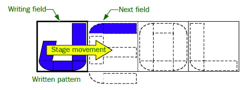
(Figure from JEOL Documentation)
These stage moves have several implications on your design, due to imperfections called “Field Stitch Errors”, which will be discussed more fully in the next page, as well as for throughput computations when choosing which lens mode to use. {Reference to Throughput computation page}
The discussion of e-beam systems continues on the next page.