E-Beam System Basics 2:
Fields and Stitches
Field Stitching
On the previous page, you learned how the beam is formed and steered on the wafer to draw shapes contained in a single e-beam field. But what if your pattern is larger than one e-beam field? Well, the system will divide your pattern into e-beam fields and write one field at a time, moving the sample stage between each field. The terminology here is to say that the individual fields of your pattern will be “stitched” together. Of course, this stitching is not perfect. I’ll try to visualize the effect for you here with this figure:
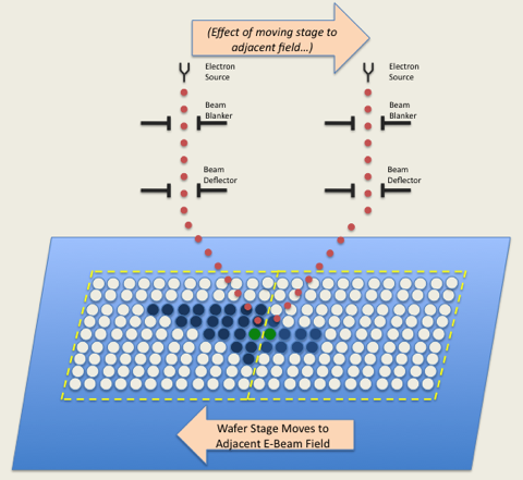
I’m showing two adjacent e-beam fields with a single blue “shape” which spans the field boundary. The system first moves the wafer stage so the the e-beam column is centered on the first field, then writes the portion of the shape within that e-beam field, as described on the previous page. The system then moves the wafer stage one field spacing to the left (which has the effect of moving the e-beam column to the right), and begins writing the remainder of that shape.
In a perfect world, the stage move would be exactly 1.00000 times the field size, and moreover, the beam placement within each e-beam field would be perfect, that is, the location of each e-beam pixel would be exactly where it is intended to be. Alas, this isn’t a perfect world, and e-beam deflection systems aren’t perfect. There will always be some placement error in positioning the beam at any pixel, and the magnitude of this error increases the further from “on-axis”, or straight down the column, the beam is steered to. So, in this sense, the error between adjacent pixels such as the two shaded in green, which are on opposite sides of a field boundary, is a worst case -- the pixel on the left is written with the beam deflected to the far right, which the right pixel is written with the beam deflected to the far left side of the e-beam field.
Another method that might be helpful to visualize these stitching errors is to think of two projectors aimed at a screen, each showing one-half of an image. The two projectors can represent the projection of adjacent fields by the e-beam onto the resist. Imagine if the image projected by one projector is shifted to the left or right, there would then be either a gap or an overlap where the two images meet -- a stitching error. Aside from a shift in one field relative to the next, this could also be caused by either a scaling error, in which a field is projected larger or smaller than its intended size, there again yielding gaps or overlaps at the stitching boundaries, or if one field is slightly rotated with respect to another, this will result in a “shear” stitch error.
Stitching Example
Let’s say we want to write a very tiny version of the U.W. logo, and at the size we want it, we need to write the logo in 4 adjacent fields, like this:
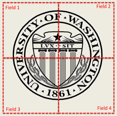
So we’ll have stitch boundaries that run halfway through our pattern both vertically and horizontally.
Now, if everything were perfect -- the substrate perfectly flat, and our e-beam being perfectly calibrated, then these stitch boundaries would be completely invisible. But, let’s say our e-beam system shows some scaling error in each field -- that is, each field is being drawn either a little smaller or a little larger than desired. The effects of field scaling (or gain) errors is shown in these two figures.
First a negative scaling error, or pattern under-sizing, leads to gaps along the stitch boundaries. Of course, if this were a circuit, not a logo, and these lines were intended to be current-carrying wires, this would be a disaster because the wires would not be continuous.

In the opposite case of scaling error with pattern over-sizing, we still have stitch errors, but now they are overlaps along the field edges. Again on the wires this would result in bulges in the width of the wires, which may or may not be harmful to the operation of your device, but are typically undesirable. In the more trivial case of our logo, it sure makes some of the words quite a bit harder to read due to the overlaps.

Finally, here’s a case where the fields have rotational error with respect to each other. Now, the stitching errors are shear errors along the axes, with lines that are supposed to line up across the boundary not even meeting!

In our real e-beam, there are always stitching errors, and those errors almost always show both imperfect scaling and rotation characters. But the magnitude of these stitching errors in our system, when properly calibrated, are very small, typically < 20 nm. Typical stitching errors are so small that we don't have any reliable way to even measure them.
For for yucks, here's the previous example in actual exposure:
![]()
Stitching Error Measurements
So what can you expect for these stitching errors?
It's very difficult to measure placement errors as small as the stitching errors our system typical produces, but here is some stitching data measurements from our system at acceptance time. These are measured using an expensive placement metrology system, a Leica I-Pro.
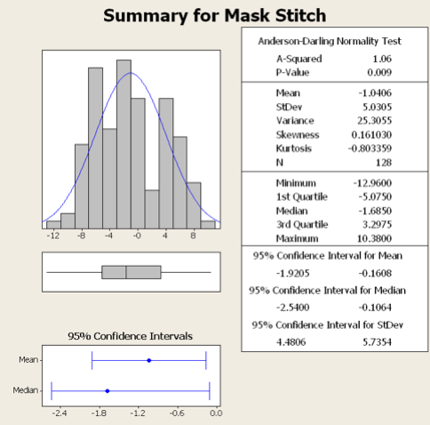
Here are a few statistics from these measurements:
| Measurement | Result |
|---|---|
| Worst Case Stitch Error: | 13 nm |
| Average Stitch Error Magnitude: | 4.4 nm |
| 1-Standard Deviation of Stitch Errors: | 5 nm |
| Stitching Error Mean + 3*Sigma: | 16.1 nm |
Now, it is important to realize these measurements are done using ideal circumstances: the system is operating at its best, calibrated perfectly, and allowed to come to complete thermal equilibrium. The substrate is an ultra-flat silicon wafer, with thin resist, exposed slowly, and the measurements are made in a small local region. So, in the real world where we try to work more quickly, our wafer might be cheap test-grade silicon, we start writing as soon as we load (so the sample temperature might not yet be fully equilibrated), and we write with a higher beam current to get our job done quickly. So as the commercial says, "Your mileage may vary." But in most cases, you can achieve stitching results not too much larger than these with more normal operating conditions.