Mark Design
The JEOL system prefers to see either a cross or an "L"-shaped alignment mark. An example of such a mark is shown here: 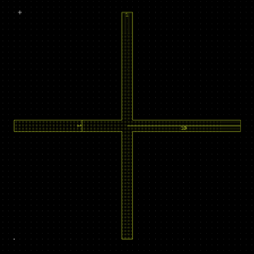
In this example, the limb width of the mark is 1 µm while the limb length is 10 µm. These exact dimensions are not essential; if you are making your alignment marks using optical lithography, the limb width could easily be 4 or even 8 µm, just to make that optical process less critical. As for the limb length, longer is better, in that it relaxes the accuracy required of your initial pre-alignment. So if you have the wafer real estate to make your limb length 100 µm long, by all means do -- you will be making your own life easier.
It is also possible to use half of a cross -- an "L" shaped mark, such as shown here:
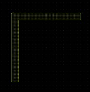
This works just fine as a local alignment mark, especially if you are using a 2-tier (global and local) alignment scheme, described in more detail below. But for your upper tier (global) alignment, having a cross is preferable, since the machine can find that a bit easier.
Finally, it is also possible, though not preferable, to use a square as an alignment mark. Due to the way the system scans the limbs looking for edges, other mark shapes will probably not work acceptably.
Mark Placement
When designing an ebeam alignment scheme, in addition to the details of the mark materials and design itself, it is important to have the marks located in appropriate locations to provide necessary alignment accuracy for your patterns, while optimizing the write time.
A first decision you will need to make is whether to do a single-tier or a dual-tier alignment. Basically dual-tier is more work, and takes longer, but results in better alignment. Unfortunately, it's hard to put numbers to "better", because (a) we can't easily and meaningfully measure alignment, and (b) the true limitation of alignment accuracy is often not the alignment scheme used, but rather secondary aspects such as mark edge roughness on the alignment marks, or placement errors on a prior layer photomask. But discuss this with the ebeam staff to make a plan. You can also include both tiers of alignment marks, but then only use the global alignment marks if you find that works well enough for your needs.
Single Tier Alignment (Global Only)
The most simple possible alignment scheme would just have two alignment marks on the substrate, as shown here:
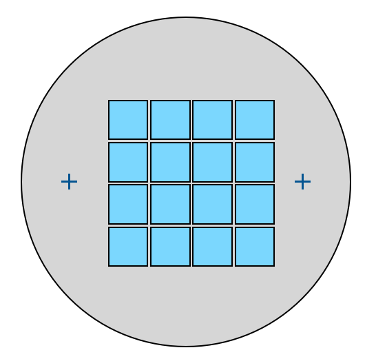
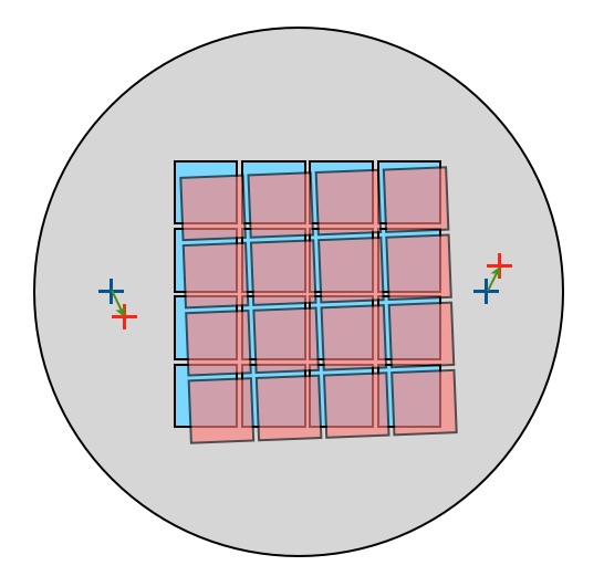
The system would then find the actual location of the alignment marks on the sample as loaded on to the stage, perhaps as shown here in red, which implies to two position error vectors shown in green:
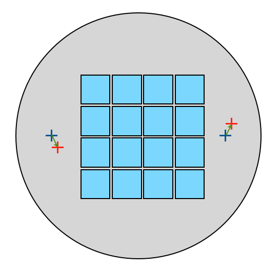
When the pattern is written, it is translated, rotated and scaled by the amounts determined by those two green mark error vectors. In ebeam, the wafer is not moved or rotated inside the system -- the alignment is corrected through purely electronic shifts and rotations to the beam scans.
A preferred, slight complication to this simple scheme is to use 4 marks instead of 2, which looks more like:
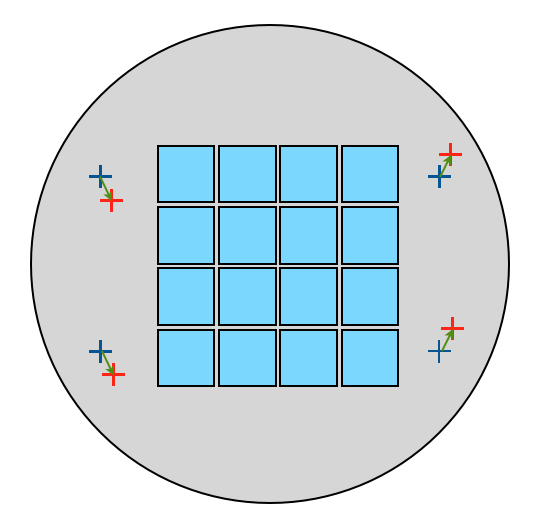
In this case, you get correction for translation, rotation, non-orthogonality (difference in rotation between the X and Y axes), as well as independent scaling and the X and Y directions. This gives the best possible alignment within the system using single-tier alignment. This sort of alignment is achieved using the SETWFR calibration routine and accompanying commands in your SDF/JDF job deck.
Dual-Tier Alignment (Global and Local Alignment)
Better alignment can typically be achieved by aligning not only the substrate, as above, but also aligning in smaller incremental regions of your pattern - perhaps individual chips or small clusters of chips, as shown in the next figure:
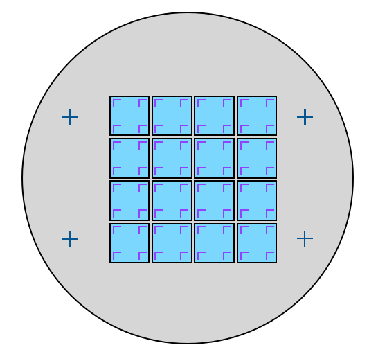
In this case, the wafer is still aligned using the 2, 3, or 4 "wafer" or "Global" alignment marks, shown in blue, but then each pattern unit is aligned using 3 or 4 "Local" or "Chip" alignment marks, shown here in purple. With each smaller unit corrected independently, alignment should be better, although that also depends on the sources of alignment error.
Other considerations
- If space is available, it can be helpful to have some duplicate, backup marks available, in case there is damage or a defect to one of your primary marks. If you do design in duplicate marks, though, make certain that the marks are distinguishable from each other, especially the first global alignment mark (which I typically confirm by SEM inspection), and as well, make sure any duplicate marks are far enough away from each other to not be accidentally located by the system. For example, in the above diagram if you had two global alignment marks very near each other, it might be possible that due to wafer rotation, the system might accidentally find the wrong mark on the far side of the wafer.
- Make sure you leave space around each alignment mark. First, so that your other features don't inadvertently confuse the system during its mark scan process. Moreover, the process of scanning an alignment mark will generally expose a large area of resist around the alignment mark scan (due mostly to scattered electrons), so any nearby features will typically be damaged by this exposure.
This image shows a global alignment mark after mark location scanning and subsequent wafer development. The large white area is where the resist has been fully exposed and then developed away. The darker long lines, two horizontal and one vertical, are heavily cross-linked resist residue where the system did long, coarse (or rough) scans over the alignment marks, and the smaller dark lines around the center of the mark are cross-linked resist residue where the e-beam system did fine alignment scans on the mark.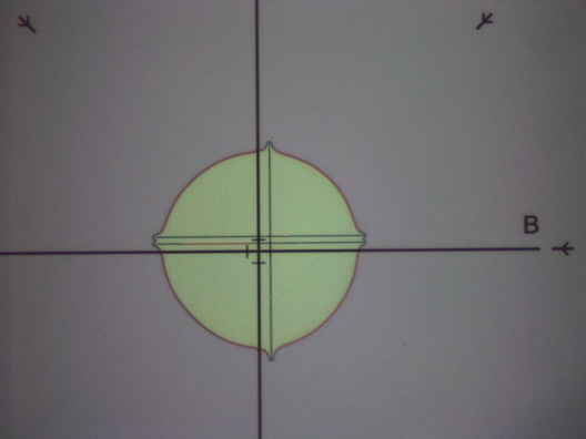
Tracking Origins, Extents, and Offsets
An essential part of setting up an alignment scheme is keeping very careful track of various positions and offsets within your layout. I highly, strongly, emphatically recommend you make a drawing to keep all of the possible offsets and positions clear.
First and foremost, you must remember that the JEOL system will place your patterns based on the CENTER of the pattern file's DATA EXTENTS. Therefore, when you create your pattern files in LayoutBEAMER, you must pay detailed attention to the pattern data EXTENT, particularly on the JEOL export module.
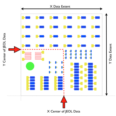
So, how is your extent determined? Well, simply put, it's the most extreme shape in each direction within your pattern data file. This has several important implications:
On a layer-by-layer basis, the data extent will vary, since each layer tends to extend different distances.
When considered on a library-wide basis, even shapes in layers OTHER than the layer you are exposing may shift the pattern extent and therefore the pattern origin.
If you edit your pattern data, you can easily shift the data extent, either intentionally or unintentionally, by adding shapes outside the existing data extent.
Within LayoutBEAMER, there are several different locations you can change the pattern extent, and different options for each.
As an example, in the above design, the yellow layer is further left than the blue layer, so if you only work on a layer-by-layer basis, each layer will have a different extent, which will shift the pattern center between each layer. This is NOT what you typically want!
I tend to use an old technique from earlier days when software wasn't as advanced or smart as LayoutBEAMER, and I draw a large bounding-box rectangle on some unused layer (I typically use Layer # 63 just for old-time reasons.) That shape then always defines my pattern extents, and I never draw outside that. And for each layer I convert, I can verify that pattern extent used matches that of the box I've drawn to define the extent. This method seems pretty simple and mostly bullet-proof.
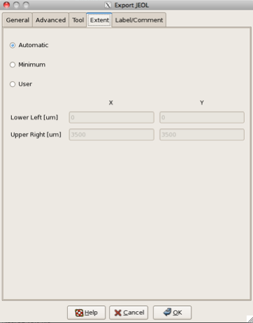
Now, LayoutBEAMER does quite an intelligent job of handling pattern data extents for you, even as you extract down data to select specific layers, and then export that data. As you can see in"Export JEOL" dialog shown here, there is an option labeled "Automatic", which generally keeps the layout extent, and therefore pattern origin consistent within a given library. (At least until you edit the library and change the data extents...)
The other options in the "Export JEOL" "Extent" dialog are: "Minimum", which as you can guess uses the minimum extent for just the data you are writing -- you generally do NOT want to use this for multi-layer aligned patterns!!, or "User", which allows manual definition of the desired pattern extents.
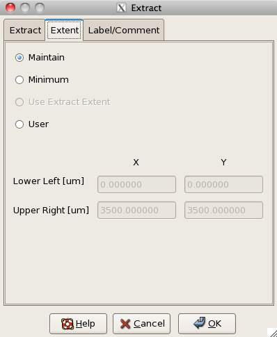
Let's back up and look at the "Extract" module, you will typically use in a flow to select out just specific layers for exposure. The "Extent" tab has an option labeled "Maintain", which will keep the data extent of the input data, all of it. Other options here include "Minimum", which will use the extent only for the layers or cells you extract, "Use Extract Extent" which is useful only if you extract just a region of your data, or "User", which allows you to manually define the extents to use.
How to know what LayoutBEAMER has done? After you run a conversion flow, specifically and EXPORT JEOL module, the "Log Info" region at the bottom of the LayoutBEAMER window will contain some important pieces of information including:
Job Frame Lower Left (x/y)[um]: 0.000000/0.000000
Job Frame Upper Right (x/y)[um]: 3500.000000/3500.000000
Bbox (in um) : (161.793, 237.618), (3425.85, 3386.66)
You should pay careful attention to the "Job Frame" numbers -- these should match the expected data extents, and the center of this "Job Frame" is where the JEOL will place your pattern file. So in this case, the (0,0) of your pattern file will be at your CAD coordinates (1750, 1750). If you place this file in your JDF layout with no further offsets, then the CAD coordinate (1750,1750) will be located exactly at the Array Point specified. (See this page for the definition of Array Points if this isn't clear.)
So, what should you do?
IF you are careful and observant, and don't plan to edit your data between layers (or be very careful when doing so), then you be pretty safe choosing "Maintain" for any "Extract" modules, and "Automatic" for any "Export JEOL" modules. But again, be sure to always verify the actual Job Frame used for each pattern layer created, to make sure they are all the same, or else you will likely have unintended pattern shifts between layers.
Another option is to always carefully specify "User" coordinates for all layers you Export; as long as you keep them consistent, all layers should then line-up as desired.
Mark Positions
There are number of offsets that you MUST be very careful about tracking and controlling, or else it's highly unlikely your patterns will land where you desire.
1) First, you must know that all substrate coordinates will be relative to the Substrate Center PLUS any additional substrate offset defined with the OFFSET command. The Substrate Center position is defined by the combination of the JOB command, which defines the substrate shape and size, and the "%" window selector, which defines which window is in use for multi-substate holders. The OFFSET command can be used to shift the virtual substrate center away from the actual holder center. This option is most commonly used with the small chip holders, where it is used to either compensate for an offset in the chip loading (ie, the chip is not loaded at the exact center of the window), or when multiple chips are loaded at one time within a single window slot.
2) Next, any pattern (Chips) are placed on your substrate using an ARRAY command, which has its own offset from the Substrate Center (above), which is entered as the first parameter in each of the X and Y definitions of the ARRAY command. The parameters you enter in the ARRAY command are the offset to the (1,1) array point element of your array, which is always the Upper Left element in your array.
This figure is intended to show the relationship between the substrate center and the Array Origin.
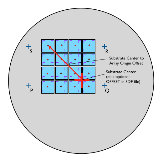
3) In order to do alignment, you must know the position of EACH global (wafer) alignment mark, relative to the Substrate Center. These are shown as the green arrows in this diagram. The JEOL software refers to your global marks as P, Q, R, and S. You'll specify these using the GLMPOS command (see below).
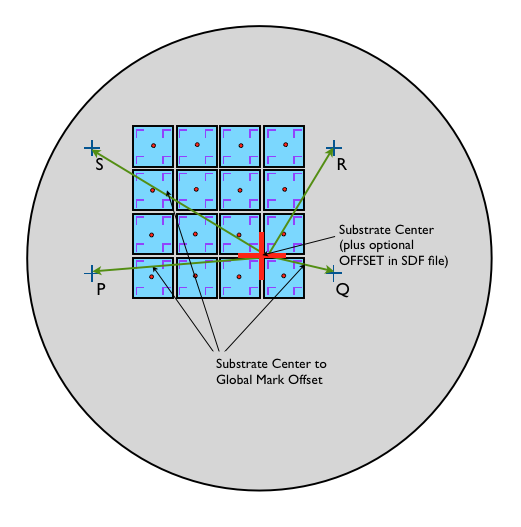
4a) If you are just doing one-tier alignment, these are the only alignment mark offsets you need to specify.
However, you must still either ensure that your pattern origin is coincident with the array point location, as discussed above by controlling the pattern extents during data preparation, or specify the desired offset from the Array Point to the center of the Pattern Data using the Offset option on the P(#) pattern definition command in your JDF file.
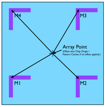
4b) If, however, you are doing 2-tier (global & local) alignment, then you must also specify the positions of the LOCAL or CHIP alignment marks. In this case, the mark positions much be specified relative to the Array Point. This location will also be the Pattern Center unless you also add a pattern offset using the P(#) pattern definition command in your JDF file. You'll specify these using the CHMPOS command (see below).
Implementation
Once your design is complete, there are then a number of steps that must be worked to execute alignment. And unfortunately, the information is scattered between the JDF/SDF files and several CALIB windows, which makes the execution of alignment seem more complicated than it should.
