Example Align Marks for EBL
This linked CAD file contains cells with recommended alignment marks for e-beam alignment, as well as examples layouts for both sample die and wafers.
There are two sets of cells within this one CAD file:
- One set contains alignment marks which use a 1 um design rule. These designs are intended to be used with the layer containing the alignment marks is to be exposed with a technology capable of readily exposing 1 um features, such as EBL or high-quality optical lithography.
- An alternate set of cells, suffixed by "_OPT" use a 4 um design rule, and thus are suitable for making alignment marks in layers with more modest optical lithography capabilities such as contact optical lithography, or low-end direct write systems.
These layouts are intended as examples, and possible design sources, but will almost certainly need to be modified and adapted to your specific needs.
GDS Layers Used
| Layer Number | Content Description |
|---|---|
| 20 | Alignment Marks (these are the marks the EBL will find and align to - so these need to be included with your prior layer, be it exposed by e-beam or optical lithography. Note that marks will be exposed, and thus are typically destroyed by the e-beam mark locate process, so you will usually need an independent set of marks for each layer to be exposed by e-beam. |
| 21 | Features to be included with your e-beam pattern exposure, which allow you to measure the overlay error of the e-beam written layer. |
| 63 | Just an outline, not meant to be exposed. Do not put any other features inside these boxes near the e-beam alignment marks, of the EBL may be confused when scanning for the e-beam alignment marks. |
Cell Descriptions
- All cell names used here are prefixed by EB_
- Be careful about modifying these cells without consulting experienced e-beam users.
- Cells that are suffixed by _OPT are intended to be exposed by optical lithography, and thus use a 4 um minimum feature size.
| Cell Name | Content Description |
|---|---|
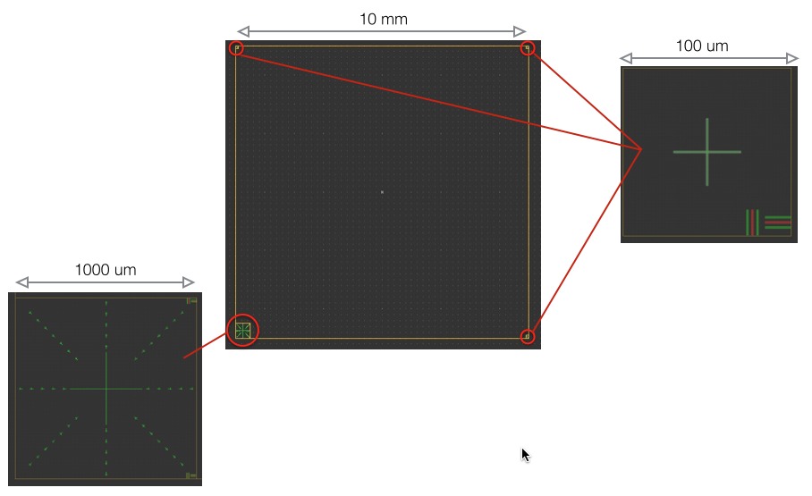
| EB_SampleDie EB_SampleDie_OPT | An example 10x10 mm die. This die contains one global marks and 3 local marks, so it has the versatility to be used for both global and local alignment, if substrate real estate is limited. (If you have the space, you can save some effort by including the larger EB_MARKS_GLOBAL_OPT cell, which is easier to locate as the limbs are larger. |
| EB_SampleDie_LCL_Only | Another 10x10 mm die, but this one contains only local alignment marks. If you place other global marks on your substrate, as in the SampleWafer layouts, then you can use just this mark for your local die, giving you a bit more space within your die for your devices. |
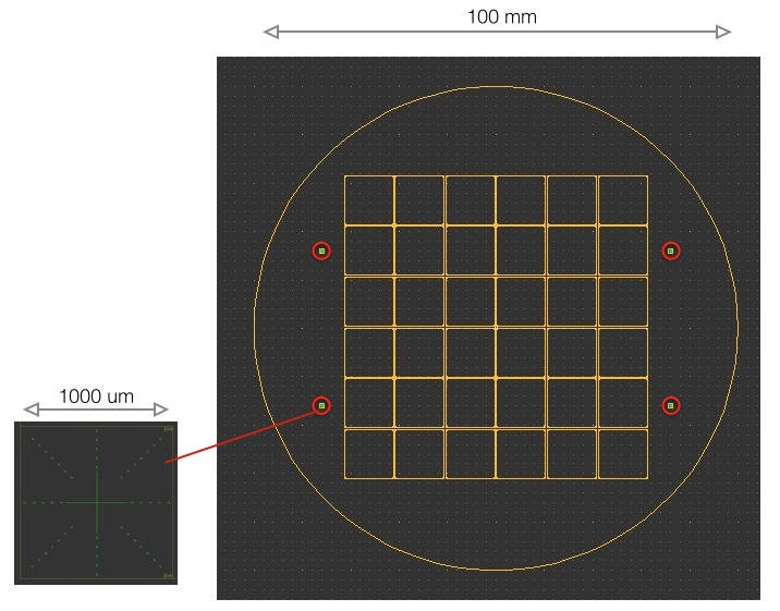
| EB_SampleWafer EB_SampleWafer_OPT | Example 100 mm wafer layout, with an array of die, and 4 global alignment marks placed at the wafer periphery. |
| EB_MARKS_GLOBAL EB_MARKS_GLOBAL_OPT EB_MARKS_LOCAL EB_MARKS_LOCAL_OPT EB_OVL EB_OVL_OPT | Sub-cells used in the above examples, containing respectively: a global alignment mark, a local alignment mark, and an overlay measurement features. Use these in your own designs, but be careful about making changes if you aren't certain of the implications. |
Images and Descriptions
EB_SampleDie and EB_SampleDie_w_gbl_OPT
This image shows screenshots of the cells for a 10 mm example die. This die contains 1 global alignment mark, in the lower left corner, and 3 marks usable as global or local marks, in the other 3 corners.
Note that is your actual chip size is 10 mm, this design will likely need to be modified so that the marks are not located so close to the chip edges -- those areas are usually damaged during processing from handling, resist edge bead, etch edge non-uniformities, and/or hidden during ebeam exposure.

EB_SampleWafer and EB_SampleWafer_OPT
This image shows screenshots of the cells for a 100 mm example wafer layout, with both global (wafer) level alignment, and local die-by-die alignment.

