Basic Concepts of CAD for Nanofabrication
Before we dig into the details of the layout procedure, I’m going to give a little background:
The type of CAD we’re going to be doing here, which still forms the basis of all microelectronics designs in use in every fab in the world, has the following characteristics:
- Two-dimensional
- Area-based
- Grid-based
- Multi-Layer
- Hierarchical
- Primitives
Let me explain each of these in greater detail:
Two-dimensional
Since microelectronics CAD is based on the idea that the data will be used to generate a photomask, the shapes within a CAD layout are all two-dimensional shapes, such as squares and polygons. Shapes have X and Y dimensions, but no Z. The shapes that make up your design are each defined as some number of 2-D coordinates, such as: (X1,Y1), (X2,Y2), (X3,Y3) etc.... Shapes to be exposed on your mask or wafer have area. In the case of a photomask, this area will either be opaque (eg chrome) or transparent (no chrome); whereas in direct write, after exposure and development, the area in your cad will either have resist removed (positive resist) or resist remaining (negative resist).Area-based
With your CAD drawing, you will be defining areas - most typically which areas of a photoresist (or e-beam resist) should be exposed and which areas should not be exposed. So your drawing has to be area-based. A not uncommon beginner error is to define only outlines rather than areas, with the mistaken belief that the inside areas will somehow be understood to be filled-in. This doesn't work. In this figure, the left drawing will result in only the outline being exposed (if anything - it's possible the outline is too narrow to be exposed at all!), versus the right shape, in which the entire, filled polygon area will be exposed.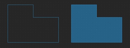
Grid-based
All data points within a design are positioned on a fixed-spacing square grid of points in 2-dimensional space. For our ebeam, this grid size is typically 1 nm or 0.125 nm. Each vertex in your shape must be located at integer multiples of this fundamental grid. If you use an exposure tool with less resolution, all vertices will be rounded (snapped) to the nearest vertex in that instrument’s grid. For some mask shops, the price for a mask build may depend on how fine the placement grid you need for your design, with finer-spaced grids costing more.Multi-layer
Occasionally something we want to build is simple enough to just be built with one layer of lithography, but more commonly, we need to build multiple layers, one after the other. So our CAD drawings accommodate this by having multiple layers within each drawing. Each shape within your drawing is assigned to exactly one layer. In the actual data file, layers are assigned a numerical label, from 0-255 (but there are several different upper values in use...) Many CAD systems also allow you map meaningful names, such as "Source", "Drain" and "Gate" to your layers (these would be layers you would find in a design for a Field Effect Transistor). But be aware that in the fundamental format, the layers will always be referenced by their number, so in data preparation for e-beam or mask writing, you'll need to know the actual data layer number(s) for the layers you wish to print.Hierarchical
A very simple CAD program might let you define shapes as described above, but to build up a more complex layout, you would have to define each and every shape individually. This would be very tedious and inefficient. A hierarchical CAD program allows you to group shapes together into “cells”, sometimes called “structures” or “blocks”. Then you can place a copy of the entire grouping of objects at multiple locations in your layout. And each cell can contain instances of other cells, so it is possible to build up a very complex layout of simple, repeated elements. On the following pages, there are several examples of Hierarchical Design.
Primitives
All designs are built up from very simple primitives, basically just 6 different types of elements. These are each described below. From just combinations of these simple elements, you can build designs as complicated as microprocessors - really! With so few simple elements, it is important, though, that you understand just what they are and how the work. Each is described in the next section, below.
Summary
It's pretty important that you grasp these principles, or you'll likely have a hard time achieving success with your CAD. Work through the following descriptions and examples, and try to ensure these principles are clear. If not, perhaps ask some more experienced users or perhaps someone from the WNF staff to try to explain to you a bit better.
Layout Primitives
Even the most complex layouts are built up from a very simple set of primitive objects. Layouts built in LayoutEditor, and all GDS-II layouts in general, contain just 6 different primitives. Let’s now look at each possible primitive object (the next section will step through creating and editing these objects -- for now, I’m just showing you what they are.)
Box
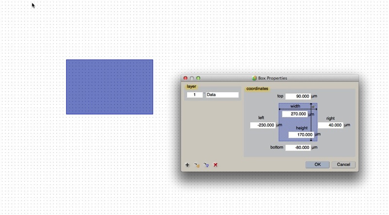
A box is described by just two (X,Y) coordinate pairs, and a layer specification. The figure shows an example. The box, which is on data layer 1, has lower left corner at (-230,-80) and upper right at (90,40). LayoutEditor also gives you the Width and Height, That’s all there is to it!
In this figure from LayoutEditor, you see box itself, drawn with a background grid. On the right side of the figure is LayoutEditor's “Object Properties” dialog window. As you can see, you can edit the vertices and layer assignment in this box. LayoutEditor also provides the convenience of displaying the box’s Width and Height for you. (For now, don’t worry about the other options shown in the lower left of these dialogs.)
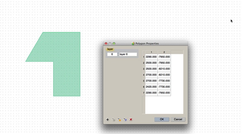
Polygon
A polygon, also called a Boundary in some CAD systems, is only slightly more complicated than a box. As you can see in the figure, a polygon is specified as a layer and a list of coordinate points which define the outline of a closed shape. You can define very complex shapes as polygons, but with the increased complexity comes more rules and limitations. I’m not going to get in to those just yet, but some advanced details about polygons are over here on the details page...
Path
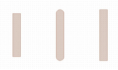
Paths are not nearly as commonly used as boxes or polygons, but they can be useful in some cases. A path is defined as a layer, a width, and a list of points. The points define the center line of the shape and the width is evenly split on either side of that center line. In other words, the path width, 2 microns in this example, is the full width of the path, so there is 1.0 um on either side of the center line.

There is an additional option for paths, but you need to be careful with this one, because some systems you might send your GDS-II pattern data to might or might not support each of these options. The option is called "Cap", or sometimes “Extension Type”, and it controls how the ends of the path are formed, and there are 3 options: None (Flush), Round, and Square (Extended). The figure shows None, Round, and Square, from left to right, so you can see how they each behave. I’ve found all 3 path types seem to work with BEAMER, so JEOL ebeam users should be ok choosing any type. Again, beware, different programs interpret path end types differently! The most common denominator is the “Flush” end type, so if you stick to that one, you’re likely safe.
Text
It’s nice to be able to put labels inside your drawing. But, there are two very distinct sorts of labels.
A: Labeling text in your design: In this case, you want labeling text just to identify different sections of your pattern as you work on your drawing.
B: Labeling text on your wafer: In this case, you actually want text to be written on your wafer, to identify items on the wafer, for example, in inspection or testing. Well, GDSII supports text, but it is really intended for the former case -- just as a reference within your drawing while you’re sitting at the CAD screen. For almost all CAD data conversion applications, the TEXT defined as GDS-II text objects is ignored and will not be written on your wafer or mask. The way to make text on your mask or ebeam writing is to make polygons in the shape of your text letters. This is easy to do in LayoutEditor, by selecting the text object and choosing "Convert to Polygon...". The resulting polygons will be exposable shapes.
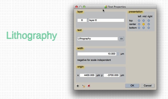
The text object is specified with a Layer #, a text string, a width (size), an (X,Y) origin coordinate, and a presentation (or justification). Again, be aware that by default, text is NOT exposed in most systems, but it is handy to use in your designs.
You can also choose the font in the LayoutEditor preferences. Finally be aware that LayoutEditor, by default, uses what's called "Scale Independent" text, which is intended only for use in labeling within your CAD file, so if you want the text be exposed on your wafer, you should set the size to some positive width - the size of your intended text.
Instance
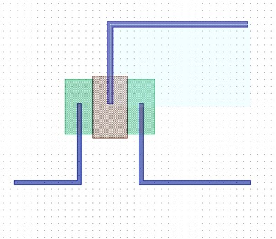
An instance is the object by which we create hierarchy in a design. First, let’s say we have a cell called “Cell1” as shown in this figure (the details on how to create this cell will be shown in the next page). In this example. the cell “Cell1” contains 6 objects, 3 boxes and 3 polygons, and these objects are on 3 different layers shown in different colors.
And now we look at an instance, or CellRef, of that cell:
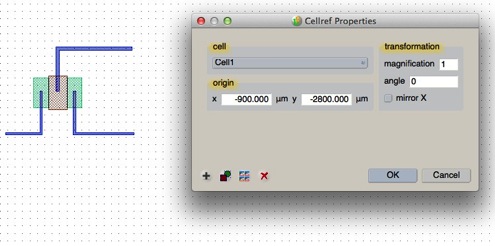
In this case, from the properties dialog we see that we are “instantiating” (fancy word for “putting”) the cell called “Cell1”, at the position (-900,-2800). There are also options for scaling (magnification), rotation angle, and mirroring, but those are more advanced.
Finally, we can place an array of these cells as a single element, a CellRefArray.
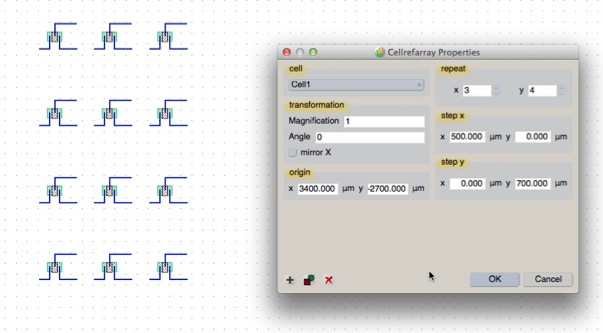
In this case, I’m not placing just a single instance of the cell “Cell1”; instead, I’m placing many instances of this cell in an array. In this example, there are 12 placements of “Cell1”, in an array 3 across (columns) by 4 down (rows), with a spacing of 500 microns in both X and 700 microns in the Y direction, with an array origin at (3400, -2700). Again, there are also options for scaling (magnification), rotation angle, and mirroring.
If you’re comfortable with this basics, continue to the next page where we’ll step through creation of a layout in LayoutEditor.