Example 2 using LayoutEditor: Transistors & Ring Oscillator
For this example, I’m going to step through building a very simple, nonfunctional electronic device, a “Ring Oscillator”, which is a bunch of transistors connected with some metal wiring. I’m assuming you know how to do the mechanics of creating layers, cells, and objects as described in the first example. The point of this example is not to teach about electronics devices, but to show more the utility, features, and capabilities of LayoutEditor in the typical type of layout work we do.
First, I’m starting with a blank layout, and I’ve created 4 layers: p_implant, n_implant, metal, and via. I’ve also set the layers to have different colors and fill patterns, but of course, that’s just a viewing preference (and I describe how to set layer appearance at the bottom of this page.) (And don’t worry if the electronics design reasons for these layer names aren’t meaningful to you, unless of course, you are a device designer, in which case, you should know these terms, or else be worried :)
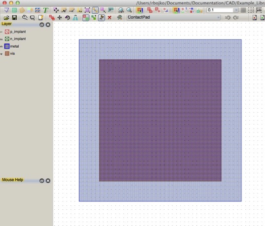
Next, I define the simplest element in my simple circuit, in this case, a cell, which I’ve called: “Contact Pad”, which is a square of metal with a “Via” hole underneath (in microelectronics, a “Via” is the term for a hole that is etched through an oxide layer to allow different layers of metal to interconnect, much like wiring in a large-scale multi-layer printer circuit board.)
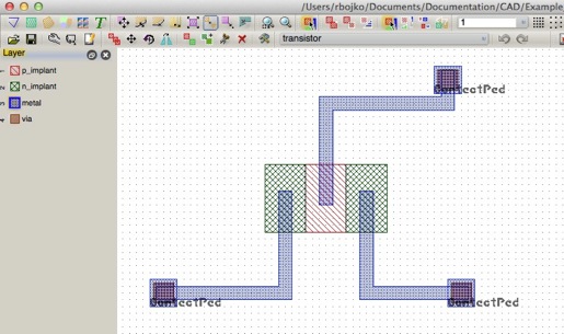
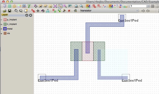
Next, I design the transistor itself, by creating a new cell, called not surprisingly “transistor”, which contains some P and N-type implants, and some metal connections, shown in red, green and blue respectively, and then three instances of the cell “ContactPad” that I created just above. These ContactPads form the input and output terminals of this transistor with which this transistor will be connected to other elements in my mini-circuit.
Note that the visibility of various levels of hierarchy is adjustable in the Settings/Preferences. If I set the Display : Drawing : CellRefs : Show Cells to off, then I no longer see the contents of sub-cells in my hierarchical layout, but instead see only the outline & name, assuming I have "Show Name" checked. As you might guess, if I also uncheck "Show Name", then I won't see the name either. Below is the exact same view, but now with the setting: Display : Drawing : CellRefs : Show Cells turned off: Now the Contact Pads are shown only as a cell outline; the details of what is inside the cell outline is not shown. An alternative, faster way to access these display settings affecting hierarchy viewing, along with other useful display options, is to right-click on the 'Operation Timer' section down in the bottom center of the LayoutEditor window, and choosing Display Cells... from the popup menu.
It is important as you build up hierarchy that you understand that you control how many levels of the hierarchy are displayed, and whether you see the details, just an outline, or nothing at all for child cells. The data is all still there, it's just visible or hidden as you choose.
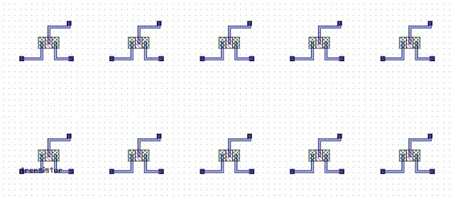
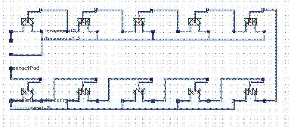
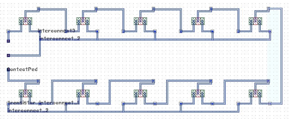
Now, continuing on my Ring Oscillator build, now that I have a basic building block transistor designed, I create another new cell called “RingOscillator”, and in this cell, I place an array 5x2, of the “Transistor” cell, which looks like this (assuming I have the View Levels set to show the details within the cells I’ve arrayed.)
Now I create some smaller cells which contain repeated interconnect wires which connect the different transistors. Each of these wires is created in its own separate cell, and each is placed in an array instance to connect different terminals from the adjacent transistors, as shown below
Finally, I add a few non-arrayed special pieces of writing, such as the input/output terminals on the left-center of the oscillator, and the lower-to-upper bus bar on the right side. So when I view the final RingOscillator cell, it now looks like this:
OK, so now we have a reasonably complex design, with 4 different lithographic Layers, and 3 Levels of data hierarchy. To reinforce the important concepts behind both design Layers and data hierarchy Levels, let's look at this design a few different ways.
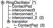
First, let's look at the "Tree" of cell names:
(You can see this hierarchy of a data library by choosing menu Cell : Select Cell... )
The indentation here is indicating the hierarchy, so the cell RingOscillator contains the other 5 cells, and then in turn the cell transistor contains 3 placements (CellRefs) of the cell named ContactPad.
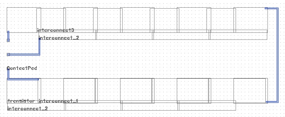
First, let's step through the view options for the data cell hierarchy. I reduce the view level to 0, by unchecking the "Show Cell" option, and here I see only the outline and identification (cell name) for each sub-cell in this hierarchy. I also see the pieces of interconnect metal (blue) that are not hierarchical, but are used to interconnect the hierarchical pieces.
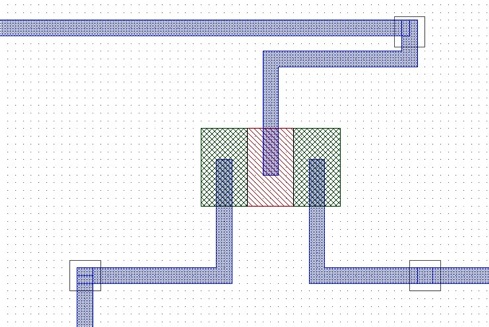
And if I set "Show Cell" to on (check the box), but the depth to 1, I see:
This looks almost like the full view shown a few figures above; the only difference is in this view, the contents of the sub-sub-cell ContactPad are not shown (which is admittedly hard to tell at this magnification. So let's zoom in a bit:
Here's a zoom with the view depth set to 1 level:
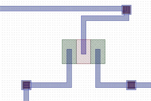
And here's the same zoom view with the Display Depth set to Unlimited. You can now see the content of the cell ContactPad, which, in the tree diagram above, is located in the second level down in the cell hierarchy.
OK, we’ve moved pretty quickly from just starting out, to a reasonably complicated, hierarchical device layout. Hopefully you are following along, and this is making some sense. Don’t get too concerned if it’s all still a bit confusing; there’s a steep learning curve when you’re first starting out with layout design, but sometimes you have to dive in and just start making some designs of your own to see how it all fits together. Think about using Microsoft Word or any complicated word-processor for the first time -- there are tons of features, many of which you never use, and at first, even simple tasks seem bewildering. But try things out and you’ll learn the essentials as you go.
VIEW LEVELS versus DESIGN LAYERS
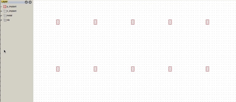
Before I move on to some more complex details, I want to show you one more set of views. The previous set of figures showed you the “View Levels” or Depths of the cell hierarchy. There is a completely orthogonal way of looking at layout: by LAYERS instead of LEVELS. Remember that LAYERs in general refer to the different lithographic steps in your device fabrication. Here’s where your wafer process and your design become integrated.Continuing with the above example of a simple ring oscillator. There are 4 lithographic layers in this example:
1) P-Implant
2) N-Implant
3) Oxide Vias
4) Metal Wires
If all 4 layers are to be exposed by photolithography, you’d have 4 unique photomasks built, one for each layer. Here are views of the cell "RingOscillator" for each mask:
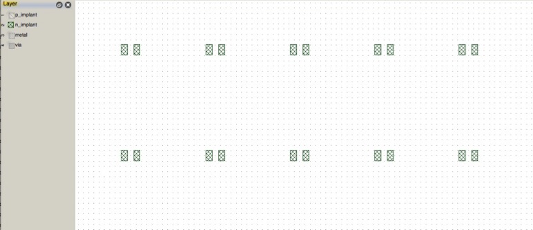
P-Implant:
N-Implant
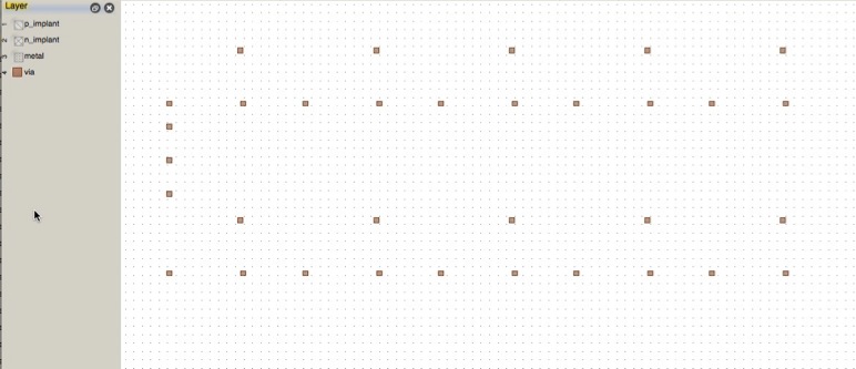
Oxide Vias:
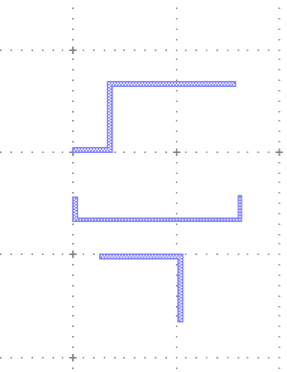
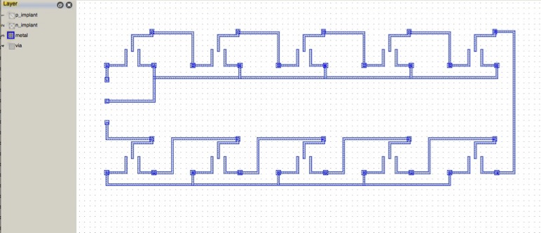
Metal:
Viewing Controls
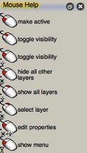
Like most everything else in LayoutEditor, you have considerable control over how your design is drawn on the screen. If you glance at the "Mouse Help" window (Lower Left Corner) while you hold the mouse over a layer in the Layer palette, you'll see some of the options that you can apply to one or more layers just with mouse clicks.
If you chose to "Edit Properties" of a single data layer, you'll see:
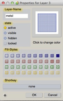
So you can set the name, pattern, color, and state (active, visible, hidden, or locked) of one layer.
There's also a "Layer Manager" from which you can define these properties for all layers:
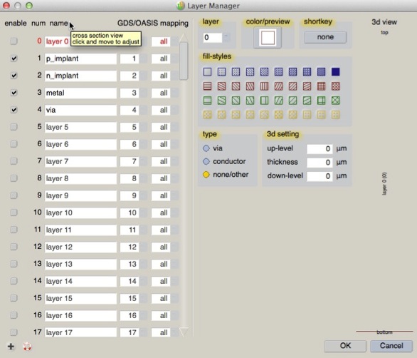
Note: Layer settings, names, colors, etc, are by default NOT SAVED in your GDSII data file, so will be lost when you save and re-open. Lousy, right? Well, don't despair: There's a setting in LayoutEditor that allows these to be saved, and thus restored when you reopen. Open the Settings / Preferences, and choose FileFormat : GDSII, and check the box next to "Store Layer Names." The layer definition information will now be stored along with your pattern data. While this is not standard for GDS-II, LayoutEditor stores this in a clever way so that it has no impact when you transfer your data file for writing on the EBL system or to a mask vendor. (It's stored in a hidden cell, as text elements and element properties, which we haven't talked about yet.)
If you’re ready for more details, the next page as a few suggestions for using LayoutEditor, and the page after that has some picky details and design advice.