SEM Inspection Sites
You may identify specific sites within your CAD design where you would like SEM images taken. To do this, designate an otherwise unused GDS-II layer to use for your SEM inspection sites, and on that layer, place a box (boundary, rectangle, polygon) at each location you would like to be imaged, with the size of the box indicating the approximate field of view.
For example, in this screen capture, the light blue box shows the desired SEM Region Of Interest.
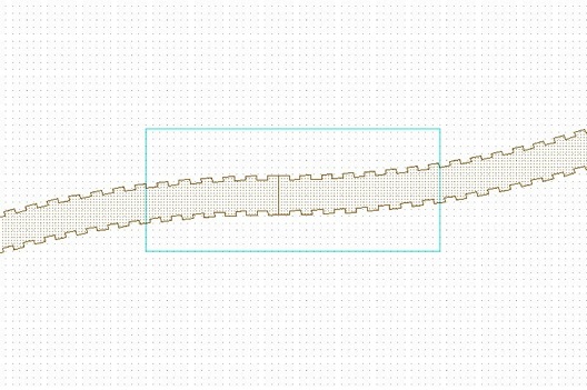
And the resulting SEM image: 
Aspect Ratio
The aspect ratio of our SEM images is: 5:4.
Image files are 1280 x 1024 pixels.
Please try to make your SEM boxes about this same ratio. They don't have to be exact, and our SEM operation is still manual so we can't match size exactly, but avoid making SEM boxes with high aspect ratios. Boxes with aspect ratios too much different from the 5:4 image ratio are ambiguous; I can't tell whether I'm better to do a closer-up or a wider-angle, so please try to keep your boxes nearly square or close to the 5:4 actual image.
Magnification Range and Recommended Box Sizes
Our SEM has a limited range of useful magnifications. Magnifications below 750X are not recommended due to excessive scan distortion at these lower magnifications. It is helpful, and saves time, if you can keep your SEM boxes to certain sizes, shown in this table:
| Field of View (µm) | Magnification (X) |
|---|---|
| 120 x 95 | 1000 |
| 50 x 40 | 2500 |
| 25 x 20 | 5000 |
| 12 x 10 | 10000 |
| 6 x 5 | 20000 |
| 4 x 3 | 30000 |
| 2 x 1.6 | 60000 |
| 1 x 0.8 | 120000 |
If you wish to compare different devices or design variants and need the SEM images to be at the same magnifications, please make sure the SEM boxes on your SEM Image Site layer are the identical size, preferably one from the table above.
Site Identification / Labeling
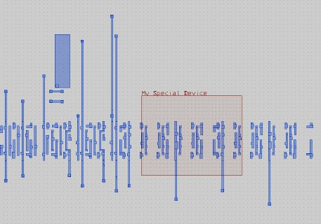
It may be helpful for you to identify your various SEM sites with some meaningful label, so that you can identify different devices, design variations, etc. The easiest way to do this is to add a TEXT element on your SEM layer at the location of your SEM site box, as shown in this figure. The image list I generate will then identify this image as being of "My Special Device". If you do include labels, please DO NOT convert these labels texts into polygons as you would otherwise have to do for the text to be exposed; please leave these labels as GDS-II TEXT elements. Alternatively, you can place your ID labels on a different GDS-II layer and give me that layer # as well. (If you convert the text elements into polygons on your SEM site layer, my extraction software will think those labels are additional SEM sites!)
Hierarchy
Be careful to not specify your SEM sites in a cell which is repeated within your hierarchy, or you will effectively be requesting a SEM image of every placement of that cell in your design, which could be very expensive for you (see time/cost below).
Arrays / Unique Structures -- Getting the exact location you want
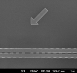
Our SEM stage navigation is generally good to within +/- 10 microns. If it isn't obvious where you want your image to be taken, for example, if you have a large array of similar-looking devices, or you have a specific location amidst many very similar-looking items, you can help insure you get the correct location and save some time by adding some sort of pointer or other indicating feature within your pattern. For example, in this SEM image, the arrow drawn in the device layer of the CAD and thus written and etched with the pattern, points to a specific object in the long array, which would otherwise be difficult and time-consuming to locate.
Time / Cost
To help you estimate costs: for most images, the tool & staff time is about 3-4 minutes per image, plus 10-15 minutes of load, setup, and unload time per chip/wafer. The current billing rates for SEM and staff time are always found at the main WNF website. Higher magnifications and challenging materials will take somewhat longer per image.