First Exposure!
Jun 25, 2010 05:37 PM
- Today, June 25, 2010, we completed the first wafer write with the new e-beam system. While this is a simple test wafer, the results look great, and work will now proceed to fine-tuning the many sub-systems and calibrating the system at several common beam conditions. For example, at this moment, the system is running a long-term static stability test, which will assess the baseline stability of many of the subsystems, including the beam generation, laser beam control, stage positioning, and thermal stability.
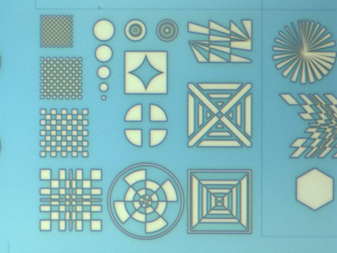
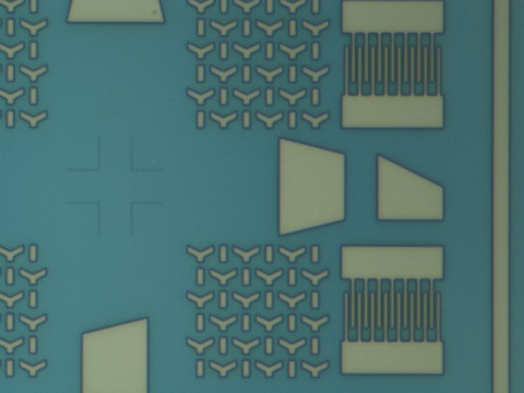
- Here are a few photos from our first wafer. The first few photos just show part of a large demo pattern that includes many different shapes.


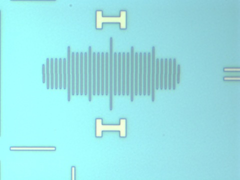
The next photo shows one of the field-stitching vernier scales. The two halves of this vernier were written in adjacent e-beam fields (500 um field size). From this photo, and the dozen or so other verniers inspected, the field stitching is indistinguishably small, at least smaller than a 20 nm error. For the “real” stitching measurements during the acceptance testing, we will ship wafers to Japan to be measured using a Leica I-Pro metrology tool, which has capability to measure stitching errors as small as our machine delivers, which measured 12 nm (Mean + 3-Sigma) during factory acceptance testing in March 2010.

